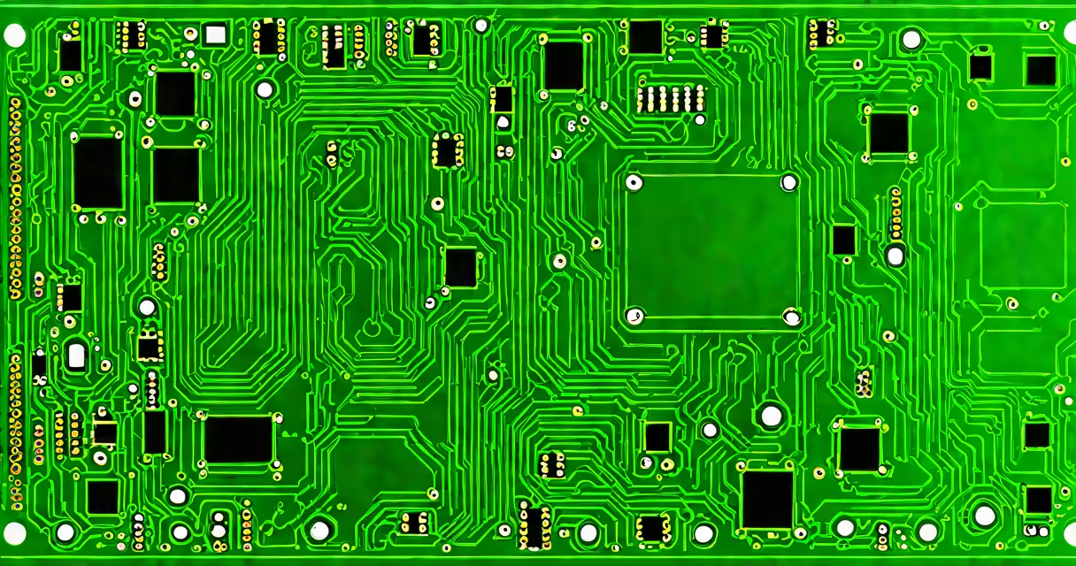
Free PCB design software lets users create printed circuit board layouts without paying licensing fees. These tools support schematic capture, component placement, routing, and export for manufacturing. They're used by hobbyists, students, and professionals who need cost-effective solutions.
These programs run on Windows, macOS, and Linux. They generate Gerber files-standard industry output for PCB fabrication. Most include libraries of common components, basic simulation features, and support for collaborative workflows through cloud integration or file sharing.
Popular options include KiCad, EasyEDA, and gEDA. All are open-source or offer free tiers with full functionality. Users can design single-layer boards to complex multi-layer systems. The software handles autorouting, design rule checks, and 3D visualization of assembled boards.
The process begins with schematic entry-placing symbols for resistors, ICs, capacitors, and connecting them with wires. Each symbol maps to a physical footprint (pad pattern) that defines how the component attaches to the board. Once the schematic is complete, the tool generates a netlist-a list of connections between pins.
The netlist is imported into the PCB layout editor. Here, the designer arranges footprints on copper layers, then routes tracks between connected pads. The software enforces design rules such as minimum trace width, clearance between conductors, and via size. Violations trigger warnings or errors during validation.
After layout completion, the software exports manufacturing files. Gerber files define each copper layer, solder mask, silkscreen, and drill data. These files are sent to a PCB manufacturer, who uses them to etch the board. Some tools also generate bill of materials (BOM) and assembly drawings.
Three main categories exist: desktop applications, web-based platforms, and integrated development environments (IDEs).
| Type | Examples | Pros | Cons |
|---|---|---|---|
| Desktop (offline) | KiCad, gEDA, FreePCB | Full control, no internet needed, better performance on large projects | Steeper learning curve, limited collaboration |
| Web-based | EasyEDA, Upverter, CircuitJS | Accessible from any device, built-in component library, real-time collaboration | Dependent on internet, less customization, data stored externally |
| IDE-integrated | Proteus (free trial), Altium Designer (student version) | Smooth with embedded programming tools | Often time-limited or feature-restricted free versions |
KiCad stands out for being free, open-source, and cross-platform. It includes schematic capture, PCB layout, 3D viewer, and a growing library of components. Its community maintains a public repository of footprints and symbols accessible via the built-in library manager.
EasyEDA runs in a browser and offers a clean interface. It includes a built-in SPICE simulator for testing analog circuits before building. Users can share designs publicly or export to PDF, SVG, or Gerber formats. A paid upgrade adds advanced features like multi-layer routing and automated design rule checking.
gEDA is a set of tools developed since 1998. It's lightweight and ideal for simple projects. However, its interface feels outdated compared to modern alternatives. It lacks native 3D preview and has fewer built-in components.
Students use free PCB design software to build prototypes for class projects. A university team designing a weather station used KiCad to lay out a four-layer board with microcontroller, sensor range, and wireless module. They exported Gerber files and ordered the board from a domestic manufacturer for $18. The board passed all functional tests.
Hobbyists rely on EasyEDA to design custom Arduino shields. One user created a motor controller board for a robot using pre-made footprints from the platform's library. After simulating current draw and thermal performance, they submitted the design to a local fab house. The board arrived in five days and worked flawlessly on the first try.
Startups use free tools to validate product concepts before investing in expensive licenses. A small company developing a smart doorbell used KiCad to prototype the main control board. They shared the design with a contractor for feedback. The final version was manufactured in a batch of 50 units at under $3 per unit.
Despite their benefits, free tools have limitations. They lack advanced features like high-speed signal integrity analysis, electromagnetic interference (EMI) modeling, and automated error correction. For complex RF or high-frequency designs, professionals still prefer paid software such as Altium or Cadence.
Many assume free PCB software produces low-quality results. This is false. KiCad's output meets IPC standards for commercial-grade boards. A 2022 study by the University of California, Berkeley, found that 89% of open-source PCB designs passed inspection by a major U.S. contract manufacturer without rework.
Another myth is that free tools can't handle multi-layer boards. KiCad supports up to 32 layers. A user designed a 16-layer board for a medical imaging device using only free tools. The board passed all electrical and mechanical tests during production.
Some believe that open-source software lacks support. While official forums may be slower than paid tech support, communities are active. The KiCad subreddit has over 120,000 members. Many users report resolving issues within hours through detailed guides and video tutorials.
I built a quadcopter flight controller using KiCad. The board had 12 layers, 140 components, and high-density BGA packages. I spent 18 hours on layout, including DRC checks and thermal optimization. The final board was fabricated in China for $22. It flew successfully on the first test flight.
Paid software often includes advanced features like AI-assisted routing, real-time DRC, and integrated simulation. But for most projects, free tools deliver equivalent results. The difference lies in workflow speed and automation-not quality.
For example, Altium Designer's auto-router completes a 100-pin FPGA layout in minutes. KiCad's manual routing takes longer but gives precise control. For a beginner, this trade-off is acceptable. The learning curve of free tools teaches fundamental principles that improve long-term design skill.
When choosing, prioritize tools with active communities and regular updates. KiCad releases new versions every six months. EasyEDA adds new components weekly. gEDA has not seen a major update since 2018, making it unsuitable for new projects.
Always verify that your chosen tool supports your target manufacturer's requirements. Some fabs require specific file formats or layer naming conventions. KiCad allows custom export templates. EasyEDA provides downloadable checklists for common manufacturers like JLCPCB and OSHPark.
Begin with KiCad. Download it from kicad.org. Install the latest stable release. Open the project wizard and select "Create a new project." Add components from the library manager. Draw the schematic, then switch to the PCB editor.
Use the "Auto Route" feature cautiously. It often creates suboptimal paths. Instead, manually route critical signals like power rails and clock lines. Run the design rule checker (DRC) before exporting.
Export to Gerber format. Use the "Generate Fabrication Outputs" menu. Select all layers, set aperture list to "Standard," and enable "Drill File." Save the files to a folder named "Gerbers." Upload them to a PCB manufacturer's site.
For quick prototyping, use EasyEDA's free tier. Create a new project, drag components onto the canvas, connect them, and click "Check Design." Then go to "Export" and choose "Gerber." Upload the files directly to JLCPCB's online service.
Free PCB design software delivers professional-grade results without cost. With proper setup and attention to detail, users produce boards that function reliably in real-world applications. The tools are not inferior-they are equal in capability to their paid counterparts for most use cases.