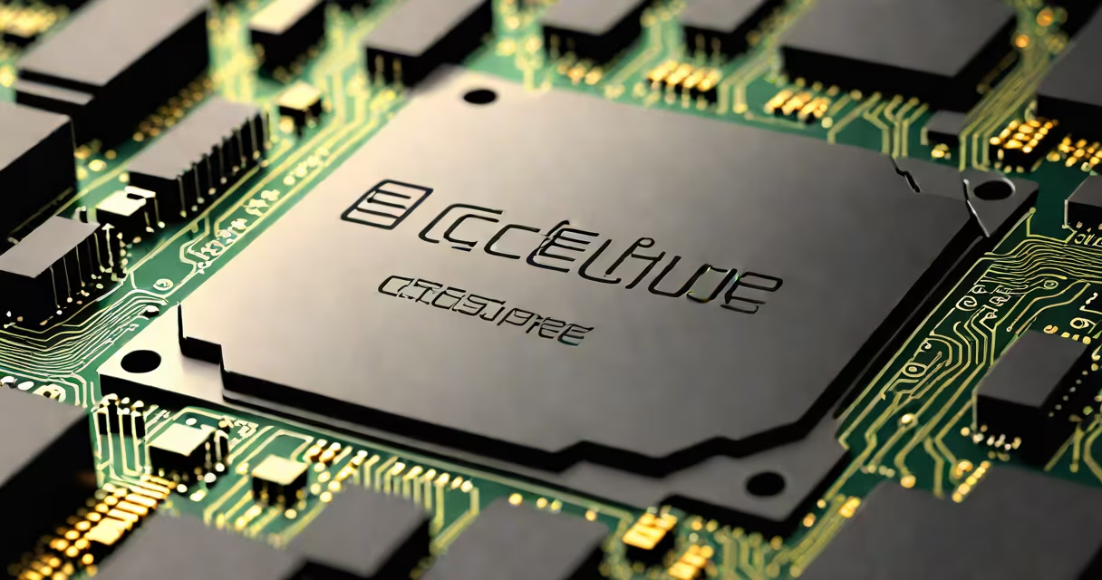
The parts of a CPU are the control unit, arithmetic logic unit, registers, cache memory, and execution pipeline-each responsible for specific stages of instruction processing within a microprocessor.
A CPU processes instructions by fetching them from memory, decoding their meaning, executing operations, and storing results. This sequence happens in nanoseconds across specialized internal components. The control unit manages data flow and coordinates timing. The arithmetic logic unit performs mathematical and logical operations. Registers hold temporary data during computation. Cache memory stores frequently accessed instructions and data. The execution pipeline enables overlapping instruction processing for speed.
Modern CPUs integrate billions of transistors across multiple cores. Each core contains its own ALU, control unit, and cache hierarchy. A single processor may have four to 64 cores depending on design and purpose. High-performance chips like Intel's Core i9-13900K or AMD's Ryzen 9 7950X use advanced packaging and interconnects to link these units efficiently.
The control unit (CU) directs the operation of the CPU. It decodes machine instructions, generates timing signals, and routes data between components. For example, when a program tells the CPU to add two numbers, the CU interprets the command and activates the correct circuits.
The arithmetic logic unit (ALU) performs basic calculations such as addition, subtraction, bitwise AND/OR, and comparisons. A 64-bit ALU can process integers up to 2^64 in size. Modern processors often include multiple ALUs per core to handle parallel operations.
Registers are small storage locations inside the CPU. They hold operands, intermediate results, and addresses. The program counter (PC) tracks the next instruction to execute. General-purpose registers store variables during function calls. Specialized registers like the flag register indicate outcomes such as zero or overflow.
Cache memory reduces delays caused by accessing main RAM. It exists in levels: L1, L2, and L3. L1 cache is fastest and smallest-typically 32 KB per core. L2 ranges from 256 KB to 1 MB per core. L3 is shared among all cores and can reach 32 MB in high-end processors.
When a program requests data, the CPU checks L1 first. If unavailable, it moves to L2, then L3, and finally main memory. This hierarchy prevents bottlenecks. For example, a video editing application loading a 4K frame may access the same pixel data repeatedly. L1 cache keeps that data close, reducing latency from 100 ns to under 1 ns.
Intel's Smart Cache technology allows changing sharing of L3 cache between cores. AMD's Infinity Fabric enables similar coordination across chiplets in Ryzen processors. These designs improve efficiency in multi-threaded workloads.
The execution pipeline divides instruction handling into stages: fetch, decode, execute, memory access, and write-back. Each stage operates concurrently on different instructions. This technique, called pipelining, increases throughput.
For example, while one instruction is being executed, the next is being decoded, and another is being fetched. Without pipelining, each instruction would wait for the previous one to finish. With it, a new instruction completes every clock cycle-even though individual instructions take multiple cycles.
Pipelining introduces hazards. Data hazards occur when an instruction depends on a result not yet available. Control hazards happen when branch instructions disrupt the flow. Modern CPUs use techniques like out-of-order execution and speculative loading to resolve these issues.
CPU architectures differ in how they organize components. x86 and x86-64 are dominant in desktops and servers. ARM architecture powers most mobile devices due to low power consumption. RISC-V is an open-source alternative gaining traction in embedded systems.
| Architecture | Use Case | Key Feature |
|---|---|---|
| x86-64 | Desktops, servers, laptops | Complex instruction set (CISC), backward compatibility |
| ARM | Smartphones, tablets, IoT | Reduced instruction set (RISC), energy efficiency |
| RISC-V | Custom chips, research, edge computing | Open standard, modular design |
Each architecture uses different combinations of components. x86 processors rely heavily on microcode to translate complex instructions into simpler ones. ARM chips use fewer transistors per instruction, enabling longer battery life. RISC-V allows developers to build custom instruction sets tailored to specific applications.
People often confuse CPU cores with threads. A core is a physical processing unit. A thread is a software-level task managed by the operating system. Hyper-Threading (Intel) and Simultaneous Multithreading (AMD) allow one core to handle two threads simultaneously-but not independently. This improves multitasking but doesn't double performance.
Another error is assuming higher clock speeds always mean better performance. Clock speed measures cycles per second (GHz), but real-world speed depends on IPC (instructions per cycle). A 3.5 GHz processor with high IPC can outperform a 4.5 GHz model with low IPC. For example, AMD's Zen 4 architecture achieves ~25% higher IPC than previous generations.
Some believe that larger cache sizes automatically improve speed. While cache helps, poor memory bandwidth or inefficient algorithms can limit gains. A benchmark test showed that increasing L3 cache from 16 MB to 32 MB improved gaming performance by only 3% on average-because the bottleneck was elsewhere.
When you open a web browser, the CPU handles dozens of simultaneous tasks. The control unit fetches instructions from the browser's executable file. The ALU computes layout positions for page elements. Registers store session IDs and cookies. L1 cache holds recently accessed JavaScript functions.
As you scroll, the CPU predicts which images will load next using branch prediction. If correct, it skips waiting for memory. When a video plays, the GPU offloads rendering, but the CPU still manages audio sync and buffering. The entire process occurs in milliseconds-thanks to tightly integrated components.
For deeper insight, study the Intel Software Developer Manual or AMD's Programmer's Guide. These documents detail instruction formats, register naming, and exception handling. They confirm that even minor differences in component design affect performance and compatibility.
Knowing the parts of a CPU reveals how software interacts with hardware. It clarifies why certain programs run faster on specific chips. It also informs upgrades-choosing a CPU with more cache or better IPC delivers measurable gains over raw clock speed.